Usuari:Single-Electron transistors (SET)
Single-Electron Transistor (SET)[modifica]
The increasing relevance of the Internet-of-Things (IoT) and the healthcare applications give more relevant impact to the electronic device power consumption. For this, ultra-low-power consumption is one of the main research topics into the current electronics world. The amazing number of tiny computers used in the day-to-day world, e.g. mobile phones, home electronics and computers; requires a significant power consumption level of the implemented devices. In this scenario, single-electron transistor (SET) has appeared as a suitable candidate to achieve this low power range with high level of device integration. The main technological difference between the well-established MOSFET device and the SET lies on the device channel concept. Instead of having a conduction channel as in case of MOSFET, which is not allowing further reduction in its length; this is replaced by a small conducting “island” or quantum dot (QD) [1]. By taking advantage of the Coulomb blockade phenomenon in controlling the transfer of individual electrons to the QD. Source and drain regions are separated to the QD by tunnel junctions. The research on SET is mainly supported on “orthodox theory” based on three assumptions:
- The electron energy quantization inside the conductors is ignored, i.e. the electron energy spectrum is treated as continuous, what is valid only if Ek << kBT.
- The time (τt) of electron tunnelling through the barrier is assumed to be negligibly small in comparison with the other time scales. This assumption is valid for tunnel barriers used in single-electron devices of practical interest, where τt ~10-15s.
- Coherent quantum processes consisting of several simultaneous tunnelling events, i.e. co-tunnelling, are ignored. This assumption is valid if the resistance of all the tunnel barriers of the system is much higher than the quantum resistance (~26 kΩ), to confine the electrons to the island.
Fig. 1 shows the basic schematic of a SET device the conductive island is sandwiched between to tunnel junctions [2], what are modeled by a capacitance (CD and CS) and a resistor (RD and RS) in parallel.
-
Fig. 1. Schematic of a basic SET and its different device parameters.
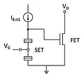
The benefits of the SET use, e.g. high integration and low power consumption, are opposed for their low current level and the low temperature operation. The thermal fluctuations can suppress the Coulomb Blockade effect; then, the electrostatic charging energy (e2/C∑) must be greater than kBT, where kB is Boltzmann’s constant and T is the temperature. This implies the maximum allowed island capacitance is inversely proportional to temperature. For this, to solve the drawback related to the SET operative only at cryogenic temperature it should be considered that an island capacitance below 1 aF is required to be room temperature operative. Island capacitance is a function of island size. In this sense, to manufacture room temperature operative SETs the island size should be reduced towards 10 nm. Besides, SET devices could be manufacture jointly with CMOS device, due to their CMOS process fabrication compatibility. Thus, it could be obtained a CMOS-SET circuit [3], [4], what it will provide larger drive current for the hybrid CMOS-SET circuits (Fig. 2).
-
Fig. 2. Schematic of a hybrid SET-FET circuit.
To highlight the relevance of the SET-based circuits the European Union (EU) concedes a project, Ions4SET (#688072) [5], that regards the feasibility of the SET-FET circuits to be operative at room temperature (RT). The basis of this project is on the design of the SET manufacturability for large-scale use of the hybrid SET-CMOS architectures. To assure room temperature operation, single dots of diameter below 5nm have to be fabricated, and exactly located between source and drain with tunnel distances of a few nanometers. Take into account that currently a reliable CMOS-compatible process of co-fabrication of RT-SETs and FETs is not yet available.
- ↑ K. Uchida, K. Matsuzawa, J. Koga, R. Ohba, S. I. Takagi, and A. Toriumi, “Analytical single-electron transistor (SET) model for design and analysis of realistic SET circuits,” Jpn. J. Appl. Phys., vol. 39, no. 4 B, pp. 2321–2324, 2000.
- ↑ [2] S. Mahapatra, V. Vaish, C. Wasshuber, K. Banerjee, and A. M. Ionescu, “Analytical Modeling of Single Electron Transistor for Hybrid CMOS-SET Analog IC Design,” IEEE Trans. Electron Devices, vol. 51, no. 11, pp. 1772–1782, Nov. 2004.
- ↑ A. M. Ionescu, S. Mahapatra, and V. Pott, “Hybrid SETMOS Architecture With Coulomb Blockade Oscillations and High Current Drive,” IEEE Electron Device Lett., vol. 25, no. 6, pp. 411–413, Jun. 2004.
- ↑ E. Amat, J. Bausells, and F. Perez-Murano, “Exploring the Influence of Variability on Single-Electron Transistors Into SET-Based Circuits,” IEEE Trans. Electron Devices, vol. 64, no. 12, pp. 5172–5180, Dec. 2017.
- ↑ M. Belli, “Ions4SET project webpage,” 2016. [Online]. Available: www.ions4set.eu.


